Achieves both high efficiency and a smaller and lower profile
Portable electronic devices such as cell phones are becoming smaller and smaller and at the same time are providing increasingly sophisticated functionality. This is accompanied by a strengthening demand for higher integration, miniaturization, and flattening of electronic components. Power ICs are no exception, as increasing miniaturization is desired.
In the case of battery-driven power, efficient use of the battery is a key issue, and a dual realization of both miniaturization and higher efficiency is becoming essential in portable electronic devices.
The high-efficiency power conversion of a DC/DC converter makes it an effective power source, however, the magnetic saturation properties of the coil and the need for burnout prevention make a low-profile design difficult, and as the IC, coil, and capacitors are generally mounted side-by-side on the board, this solution has not been suited to miniaturization.
A number of methods have been devised to solve these problems.
One method is to form a coil on the semiconductor silicon; however, to obtain an inductor value that is sufficient for use in a DC/DC converter, a complex semiconductor process must be used and a high cost results. As such, the actual use of this method is limited to devices such as high-frequency filters.
Another method is to encapsulate the coil and DC/DC converter IC in a single plastic mold package. If the components are simply inserted, there is extra mounting area left over, the size is not reduced, and little advantage is obtained.
A method was thereupon devised whereby the components including the IC are stacked rather than placed side-by-side, and a number of products have actually been created. However, a pattern for wiring is needed on the coil, a CSP (Chip Scale Package) is needed for the IC, and a mold process is needed for IC encapsulation, and thus the manufacturing process tended to be complex and expensive.
micro DC/DC XCL205/XCL206/XCL207 Series
Our “micro DC/DC” XCL series of coil-integrated step-down DC/DC converters achieves both a reduction of the mounting area and good characteristics by means of a simple structure whereby the coil is placed on top of the complete DC/DC converter IC.
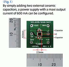
The only components that are needed to output the output current (maximum of 600 mA) are two capacitors, enabling miniaturization when mounting on the board [Fig.1].
The simple structure allows existing mass production pieces to be used without degrading the characteristics of the IC, a major advantage.
Ultra-simple structure
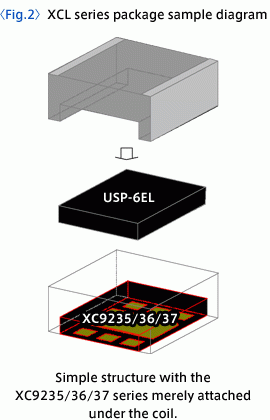
To simplify the manufacturing process of the XCL series, we developed a structure for integration of the DC/DC converter with the coil whereby a depression is formed in the center of the coil and the XC9235/XC9236/XC9237 series is inserted into the depression and affixed. This eliminates the high cost associated with a complex process [Fig.2].
This structure also makes it possible to mount the top coil electrodes and the IC pins directly onto the PCB, allowing the DC/DC converter wiring to be accomplished by means of the PCB layout.
Low profile : only 1 mm in height
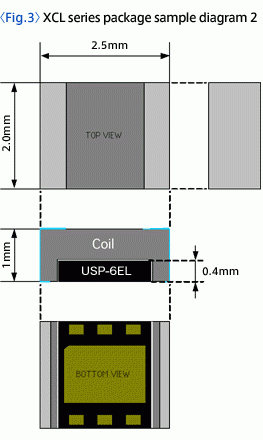
To limit the height of the combined coil and DC/DC converter to 1 mm, we developed a new ultra-flat package (USP-6EL) with a height of 0.4 mm for the DC/DC converter [Fig.3].
IC characteristics are maintained
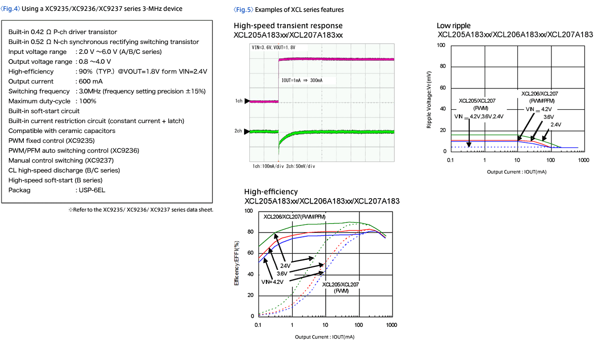
The DC/DC converter ICs used for the XCL205/XCL206/XCL207 are the XC9235/36/37 series. The main features of this series are an operating voltage of 2.0 V to 6.0 V, an output voltage that can be set from 0.8 V to 4.0 V in steps of 0.05 V, a switching frequency of 3 MHz, and synchronous rectification with a built-in 0.42 Ω P-ch driver transistor and a built-in 0.52 Ω N-ch switching transistor. Three operation modes can be selected: PWM control (XCL205), PWM/PFM automatic switching control (XCL206), and manual control switching (XCL207). A high-speed response, low ripple, and high efficiency have been achieved over the full load range from light loads to heavy loads, and the quiescent current is held to 1.0 μA or less by shutting down all circuits during standby. The built-in UVLO (Under Voltage Lock Out) function forcibly turns off the internal driver transistor when the input voltage is 1.4 V or less [Fig.4][Fig.5].
Applications
Target markets are small portable devices that require high efficiency and have limited component mounting space such as cell phones, smartphones, PDAs, handheld game consoles, digital cameras, UMPCs, and PNDs. We expect high demand for this series in the small portable devices that are becoming increasingly sophisticated with each passing year.
Details of the Products
-
Inductor Built-in
-
Inductor Built-in
-
Inductor Built-in