0.8μA Low Quiescent Current Dual Voltage Regulator
The XC6411 series are highly precise, low noise, positive voltage LDO dual regulators manufactured using CMOS processes. The series achieves very low quiescent current, 0.8μA / ch. (TYP.) and consists of a reference voltage source, an error amplifier, a current foldback circuit, and a phase compensation circuit plus a driver transistor. SOT-25 package for the XC6411P series make high density mounting possible. Therefore, the series is ideal for applications where high density mounting is required such as in mobile equipment. Output voltage of each regulators VR1 and VR2 is selectable in 0.1V increments within a range of 0.9V to 5.0V by laser trimming. The series is also compatible with low ESR ceramic capacitors, which give added output stability. VR1 and VR2 are completely isolated. For this, a cross talk between each channel, which causes a problem during load fluctuations, can be greatly reduced, and the stabilized voltage can be supplied. The current limiter's foldback circuit also operates as a short protect for the output pin.
Feature
| Maximum Output Current | 200mA(300mALimitTYP.),(VOUT=3.0V、VIN=4.0V) |
| Dropout Voltage | 320mV@IOUT=100mA(VOUT=3.0V) |
| Operating Voltage Range | 1.5V~6.0V |
| Output Voltage | 0.9~5.0V |
| High Accuracy | ±2%(1.5V<VOUT≦5.0V) |
| Low Quiescent Current | 0.8μA/ch(TYP.) |
| Operating Ambient Temperature | -40℃~85℃ |
| Output Capacitor | Low ESR Ceramic |
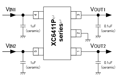
Typical Application Circuit
Quality Reports
Packages
| Package | Number of Pins | Pcs/Reel | Package Size(mm) |
|---|---|---|---|
| SOT-25 | 5 | 3,000 | 2.8 x 2.9 x 1.3 |
XC6411 Series Part Numbers
| Part number | Sample | Output Voltage | Packages | EDA | Online Store |
|---|---|---|---|---|---|
|
|
|
|
|
|
|
| XC6411P001MR-G | VR1=1.5V,VR2=3V | SOT-25 |
|
||
| XC6411P002MR-G | VR1=1.5V,VR2=3.3V | SOT-25 |
|
||
| XC6411P003MR-G | VR1=1.5V,VR2=1.5V | SOT-25 |
|
||
| XC6411P004MR-G | VR1=1.5V,VR2=2.5V | SOT-25 |
|
||
| XC6411P005MR-G | VR1=1.8V,VR2=2.5V | SOT-25 |
|
||
| XC6411P006MR-G | VR1=1.5V,VR2=1.8V | SOT-25 |
|
||
| XC6411P007MR-G | VR1=2V,VR2=3V | SOT-25 |
|
||
| XC6411P008MR-G | VR1=3V,VR2=2.5V | SOT-25 |
|
||
| XC6411P009MR-G | VR1=2.8V,VR2=3V | SOT-25 |
|
||
| XC6411P010MR-G | VR1=1.8V,VR2=1.8V | SOT-25 |
|
||
| XC6411P011MR-G | VR1=1.8V,VR2=3.3V | SOT-25 |
|
||
| XC6411P012MR-G | VR1=1.8V,VR2=2.7V | SOT-25 |
|
||
| XC6411P013MR-G | VR1=3.3V,VR2=1.8V | SOT-25 |
|
||
| XC6411P014MR-G | VR1=3.3V,VR2=3.3V | SOT-25 |
|
||
| XC6411P015MR-G | VR1=2V,VR2=2V | SOT-25 |
|
||
| XC6411P016MR-G | VR1=1.8V,VR2=1.3V | SOT-25 |
|
||
| XC6411P017MR-G | VR1=1.2V,VR2=1.8V | SOT-25 |
|
||
| XC6411P018MR-G | VR1=3V,VR2=1.5V | SOT-25 |
|
||
| XC6411P019MR-G | VR1=2.8V,VR2=1.8V | SOT-25 |
|
||
| XC6411P020MR-G | VR1=3V,VR2=3.7V | SOT-25 |
|
||
| XC6411P021MR-G | VR1=3V,VR2=3V | SOT-25 |
|
||
| XC6411P022MR-G | VR1=1.8V,VR2=3V | SOT-25 |
|
||
| XC6411P023MR-G | VR1=1.8V,VR2=3.6V | SOT-25 |
|
||
| XC6411P024MR-G | VR1=3V,VR2=1.2V | SOT-25 |
|
||
| XC6411P025MR-G | VR1=1.2V,VR2=1.2V | SOT-25 |
|
||
| XC6411P026MR-G | VR1=3.1V,VR2=3.1V | SOT-25 |
|
||
| XC6411P027MR-G | VR1=1.2V,VR2=3.3V | SOT-25 |
|
||
| XC6411P028MR-G | VR1=2.7V,VR2=1.8V | SOT-25 |
|
Inquiries About XC6411
Please wait for a while until the form is displaying.
If the form is not displaying, please contact us from inquiry form.