Charge pump
A charge pump is a circuit that increases and reverses the voltage using a clock signal, capacitor, and switch (FET or diode).
A charge pump has the following features.
Advantages
- Can be configured using just a capacitor and a switch (diode), so saves space
- Does not require a coil
- Low discharge noise
- Boost and negative voltages are possible
Disadvantages
- Cannot output a large current
- Capacitor discharge charge is used, causing a large ripple voltage
A diode charge pump consisting of a clock signal (DC/DC switching node, etc.) and a diode is often used to create a high voltage or negative voltage at low cost.
This section uses a reverse power supply creation method employing a diode charge pump to introduce the related principles and some actual examples.
Reverse charge pump circuit operation principles
The operation is explained by separating it into the charge and discharge operations to the capacitor CPUMP.
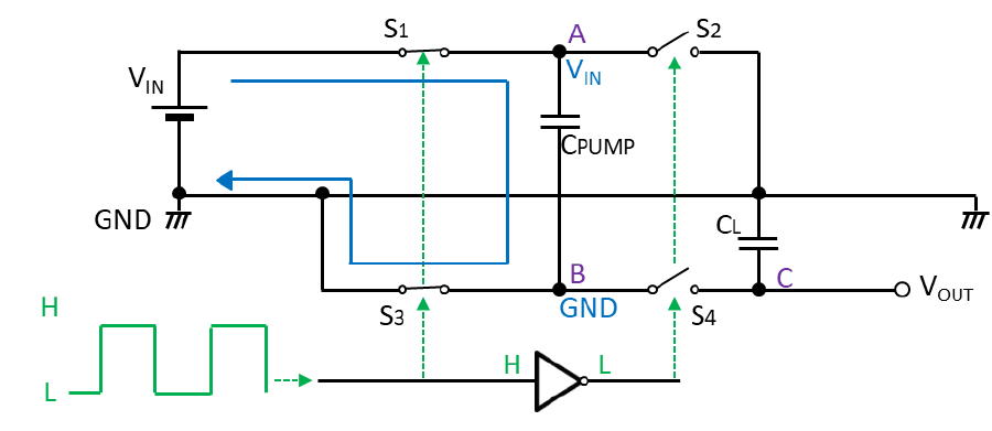
Step1: Charge operation
When S1,S3 is on and S2,S4 is off, the B point voltage becomes the GND. The current flowing in the blue wire charges until the CPUMP voltage becomes VIN to make the voltage between the CPUMP terminals become VIN.
Step2: Discharge operation
When S2,S4 is on and S1,S3 is off, the A point voltage becomes the GND. The voltage of Vin between the CPUMP terminals is maintained, so the A point voltage decreases from VIN to GND, which also causes the B point voltage to decrease from GND to -VIN.
When the B point voltage decreases to -VIN, the CPUMP discharges to the output capacity CL, causing the output voltage to decrease. (Refer to the red line.)
This operation can store a negative voltage in the output capacity CL.
Negative voltage generation circuit using a diode
This section introduces an actual negative voltage generation method that uses a diode.
With a diode charge pump circuit, it is possible to generate a -N times voltage depending on the circuit method.
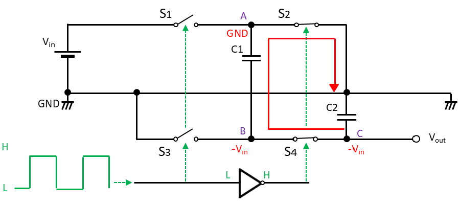
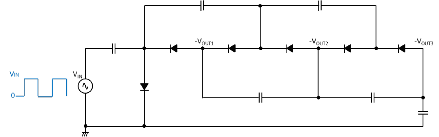
Basic circuit (1)
It is possible to output a -N(≧1) times output voltage from the clock output.
A lower voltage can be output by stacking the diode charge pump stages. There is loss from the Schottky diode at each stage, so the output voltage at N times is calculated using the following formula.
VOUT(N) = VIN × N - VF × 2(N - 1) - α
VF: Schottky diode forward voltage α: Other loss
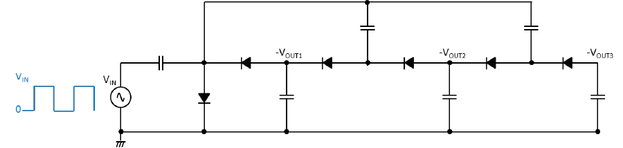
Basic circuit (2)
Compared to basic circuit (1), the startup time is quicker, but the stability is a little worse. The output voltage at N times is expressed using the following formula the same as for basic circuit (1).
VOUT(N) = VIN × N - VF × 2(N - 1) – α
VF: Schottky diode forward voltage α: Other loss
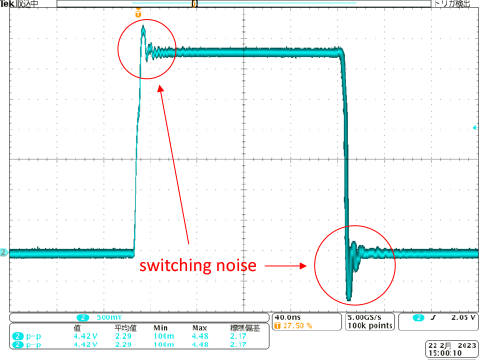
Let’s check if a negative voltage is created by the “-1 times diode charge pump” using basic circuit (1) and a DC/DC switching node.
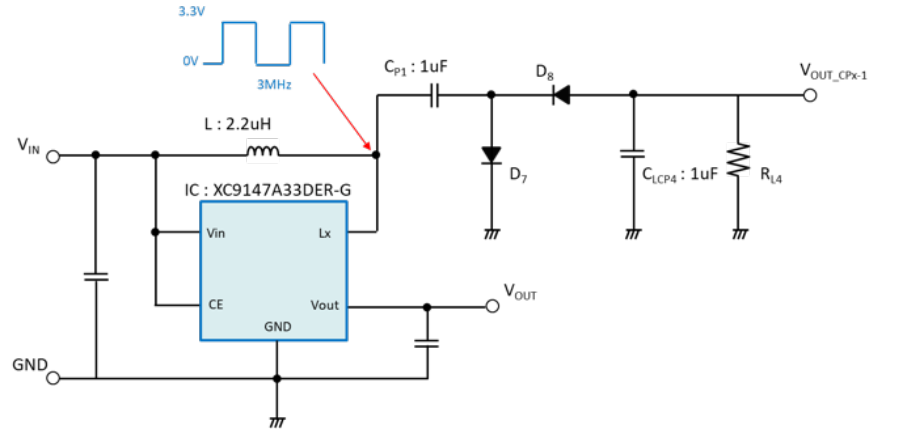
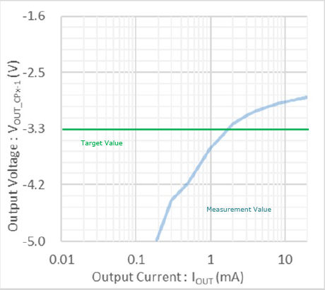
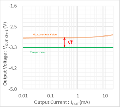
A -1 times output voltage of the input voltage is being output, but at a low load, the output voltage is higher than -1 times.
The switching noise from the DC/DC switching node contains switching noise with a high-frequency component above that of the output voltage. In the charge pump, this switching noise is also reversed, so an output voltage that is higher than -1 times is output.
Making the output current larger causes the output voltage to approach -1 times. For this reason, a general countermeasure to the rising output voltage is to connect a load resistance to the output side.