The IC internal block configuration and block roles need to be considered first to understand the operation principles of the linear voltage regulator.
The inside of the voltage regulator has a configuration that is divided into four blocks.
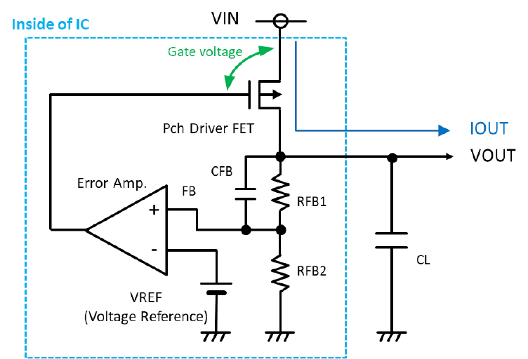
(a)Voltage Reference (VREF)
This is the voltage reference inside the IC.
This is used by the voltage regulator as the reference power supply for error amplifier comparison.
In an actual IC, the voltage reference is also used for blocks other than error amplifier.
(b)Feedback resistance: RFB1, RFB2
The output voltage is divided to create an error amplifier comparison voltage.
In an actual IC, the comparison of RFB1 and RFB2 can be changed to adjust to output the desired set output voltage.
(c)Error amplifier (Error AMP)
Comparing the voltage reference with the feedback voltage from the feedback resistance to control the driver transistor/FET to produce the desired set output voltage.
The voltage regulator conducts negative feedback control to control the driver transistor/FET so that the voltage reference and feedback voltage from the feedback resistance are the same.
This negative feedback operation adjusts the resistance of the driver transistor/FET to maintain a constant output voltage regardless of the input voltage and output current.
(d)Driver transistor/FET
This transistor/FET changes the resistance depending on the signal from the error amplifier.
Generally, many products use a Pch FET, but there are also products that use an Nch FET or PNP/NPN transistor.
This device also adjusts the resistance even if the transistor/FET types differ.