Li-ion / Polymer batteries are used in many devices, and their applications are expanding further, such as IoT, sensor devices, and wearable devices.
These chemistries require dedicated charging IC and in our example solution circuit we illustrate the different options available from Torex, in particular, we will introduce step-down DCDC for lower consumption, low-noise power supply for sensors and wireless communication, and countermeasures for equipment abnormalities such as freezes.
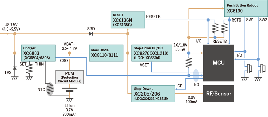
Block Diagram(a) See the Solution Summary↓

Block Diagram(b) See the Solution Summary↓
| Block diagram | Requirements | Recommended ICs | Features |
|---|---|---|---|
| Charger To charge Li-ion/Polymer |
Specifications Other points
|
XC6803 (XC6804 / XC6808) |
Linear Li-ion Charger
VIN: 4.5~6V |
| Ideal Diode For OR connection of 5V ppower input and battery power rails |
Specifications Other points |
XC8110 / XC8111 |
Ideal diode load SW
VIN: 1.5~6V |
| Step-down / LDO For MCU |
Specifications Other points
|
XC9276 (XCL210) |
Ultra-Low Quiescent Current step-down DC/DC with output voltage selectable function
VIN: 1.8~6.0V |
| XC6504 |
Low consumption CL less voltage regulator
VIN: 1.4~6.0V |
||
| Step-down / LDO For RF / Sensor |
Specifications Other points
|
XCL205 / XCL206 |
Inductor built-in step-down DC/DC, PWM (XCL205), PWM/PFM (XCL206)
VIN: 1.8~6.0V |
| XC6233 (XC6215) |
Fast transient response / high PSRR voltage regulator
VIN: 1.7~5.5V |
||
| RESET To monitor battery voltage |
Specifications |
XC6136N (XC6135C) |
Ultra low consumption RESET
VIN: 1.1~6.0V |
| Push Button Reboot |
Specifications |
XC6190 |
Push Button reboot controller
VIN: 1.75~6.0V |
Solution Summary
IoT devices powered by Li-ion or Li-Polymer batteries need a Charger IC and normally use step-down DC/DC or LDO Voltage Regulators to reduce the battery Voltage to a lower level required by the microprocessor (MCU) and peripheral IC.
The block diagram (a) shows a simple configuration example.
Battery Charger IC
Firstly, we will discuss the different types of Charger IC
When selecting a Charger IC we should consider the required Charge Voltage (CV) and Charge Current (CC). Often the CC is fixed externally using a Resistor (RISET) as shown in the block diagram. The CV is normally factory set by laser trimming.
Battery charging ICs
XC6808: CC 5mA - 40mA, CV 4.2V, 4.35V or 4.4V
XC6803: CC 40mA - 280mA, CV 4.2V
XC6804: CC 200mA - 800mA, CV 4.2V
With Li-ion or Li-Polymer batteries a PCM (battery Protection Circuit Module) is almost always required. These PCM can be intergated into the battery pack or placed on the PCB. The battery temperature can be monitored using a Thermistor (NTC) placed close to the battery on the PCB or inside the battery pack.
For smaller batteries, temperature monitoring is not always required and The Charge Status Output (CSO) function can be used to monitor the charge condition.
The CSO pin has an N-ch Open Drain Output with external pull-up resistor. The output signal will be pulled 'HIGH' to march the level of MCU I/O Voltage.
An LED can also be used to display the charge status and it is advisable to drive the LED through a current limiting resistor that is connected to VIN, to ensure the LED is not driven by the charge current supplied by the Charger IC.
Although Charger IC do include ESD diodes internally, care should be taken to protect the VIN pin because there are many brands of USB adaptors on the market and some are better than others. A poor quality adaptor can generate high voltage spikes under no-load conditions and therefore an external TVS Diode or Zenner should be implemented at the input as a countermeasure.
Step-down DC/DC and LDO Voltage Regulators for MCU
The CV for Li-ion or Li-Polymer batteries is normally around 4.2V and the maximum input Voltage for the MCU is typically 3.8V or less, so a step-down DC/DC or Voltage Regulator is required to lower the battery Voltage for use within the system.
Today's MCU can operate in sleep or standby modes for long periods of time so high efficiency is required over a wide range of IOUT conditions from a few uA during sleep mode to 100mA or more when the MCU is operating fully.
Using DC/DC with ultra-low quiescent current helps ensure high levels of efficiency when the MCU is in sleep mode and further savings can be realised by lowering the DC/DC output Voltage using a VSET function when the MCU enters sleep mode. Reducing the operating Voltage, even with the same quiescent current will significantly improve the overall system efficiency.
When normal MCU operation is required, the DC/DC Voltage will need to be increased again, because many of the standard MCU functions require higher input Voltages to operate correctly. The MCU can switch between the different Voltage levels using the VSET pin.
By varying the DC/DC Voltage in this way, we maximse the efficiency and help to prolong battery life.
Step-down DC/DCs
XC9276: Iq = 200nA, output voltage selectable function
XCL210: Inductor built-in type, Iq = 0.5μA (no output voltage selectable function)
Voltage Regulators can also be used to step-down the battery Voltage in place of a DC/DC. They are simple to implement and are generally more cost effective when compared to a DC/DC solution, however the lower efficiency and power dissipation can be a concern.
Voltage regulator
XC6504: Iq = 0.6μA, output capacitor unnecessary
Step-down DC/DC and LDO Voltage Regulators for RF & Sensors
Radio IC and Sensors also typically operate a lower Voltages, so DC/DC and Voltage Regulators are often used for their power supply.
For Radio IC the power solution must normally deliver a clean Voltage with low noise and low EMI.
Step-down DC/DCs
XCL205: Inductor built-in type PWM, 3MHz / high efficiency / low EMI
XCL206: Inductor built-in type PWM/PFM, 3MHz / high efficiency / low EMI
The MCU will normally control the operation of the Radio IC and Sensors, turning them ON and OFF as required. This is normally achieved by controlling the CE pin of the DC/DC or Voltage Regulator powering the Radio IC or Sensor.
By controlling the operation via the DC/DC or Voltage Regulator, the user not only saves the power used for the Radio and Sensors, but we also turn off the power IC to concerve energy and prolong battery life.
A DC/DC with fixed frequency PWM mode ensures maximum efficiency at higher output loads and offers the lowest output ripple with easier noise management.
Alternatively PFM/PWM automatic switching can be used for improved efficiency during light loads. DC/DC with built-in inductor are also available, offering better EMI suppression and smaller PCB area.
As a general rule, if Voltage Regulator is used, a high speed LDO Regulator, with high Power Supply Ripple Rejection (PSRR) and fast load transient response should be chosen to ensure a clean supply.
However, if the output noise at higher frequencies (>100kHz) is an important consideration, then a low power LDO with lower IQ may be more suitable because their output noise can be surprisingly low at high frequencies.
Voltage regulators
XC6233: High speed
XC6215: Low power
RESET IC
Also know as Voltage Supervisors or RESET IC, these IC are used to monitor a voltage rail or battery level.
If the Voltage being monitored is at a different level to the MCU's supply Voltage a Voltage Detector with N-ch open drain output and an external pull-up resistor can be used. If the Voltage levels are the same then Voltage Detector with CMOS output can be used without any resistor.
To avoid the quiescent current associated with the N-ch output's pull-up resistor, an alternative method is to use a Voltage Detector with a VSEN pin separated from VIN. If the VIN level is the same as the MCU a Voltage Detector with CMOS Output can be used and the Voltage being monitored is connected to VSEN.
Voltage detectors
XC6136 Type N: Iq ~ 100nA (Type N: Nch open drain output)
XC6135 Type C: Iq ~ 100nA, sense pin isolation type (Type C: CMOS output)
Push-button reboot controller
These IC are added to a circuit as a countermeasure against system freezes (when the system ceases to respond to inputs, due to an unforeseen software or hardware error)
Push-button reboot controller
XC6190
Modern Li-ion and Li-Polymer Batteries are not normally accessible to the user, so they cannot easily be disconnected from the system to force a reset. As a result, reboot controller IC are now commonly used to perform this reset function.
In the example circuit we show two external push-button switches which are used to control the MCU in conjunction with the Push-Button Reboot Controller IC.
After a system freeze, the user can initiate a full reset by pushing and holding down both push button switches for a predetermined period of time. This action makes a RSTB "L" signal which is used to instruct the MCU to initiate a full system reset.
In our circuit, RSTB is connected directly to the MCU, but the signal could also be used to drive the CE pin of the main system power supply IC, which is another method of resetting the system (turning the power off and on).
Ideal Diode Load SW
The block diagram (b) shows the case where the power rails from the 5V and Li batteries are separated and OR-connected. It is suitable for cases where the system consumes a lot of current during charging and cases where a Li battery is used as a backup.
Generally, SBD is used for OR connection, but the voltage drop of 0.3 to 0.5V due to its Vf becomes a loss, which greatly affects the device usage time and backup time when operating with Li batteries.
The ideal diode load SW has a very small Vf equivalent of 20 mV, so the loss is small and it is ideal for long-term battery use.
A usual load switch with reverse current prevention can only be stopped after a certain amount of reverse current, and could not be used as a substitute for SBD. On the other hand, the ideal diode load SW always prevents reverse current so it's suitable with batteries.
Ideal Diode Load SW
XC8110: 500mA
XC8111: 1A
As described above, placement of ICs with the most appropriate functions will make it possible to construct high-performance but simple devices with low noise and long life required.