Here explains basic usage of DC/DC simulation and how to confirm the basic characteristics.
Confirming simulation and simulation result in a method shown here can be utilized for "prediction of characteristics before making an actual machine", "selection of an optimum IC", and "validation of pilot experiment result", etc.
1. Basic usage
The simulation can be executed by just inputting the power supply specifications to be simulated for the input items.
If you change the power supply specifications, the simulation result will be automatically output. It is possible to confirm the desirable characteristics by selecting a tab according to the characteristic you want to confirm.
Step 1. Select a product
Step 2. Select oscillation frequency
Step 3. Select an operation mode
Step 4. Input the power supply specifications (Vin / Vout / Iout / peripheral component values etc.)
Step 5. Confirm the simulation result
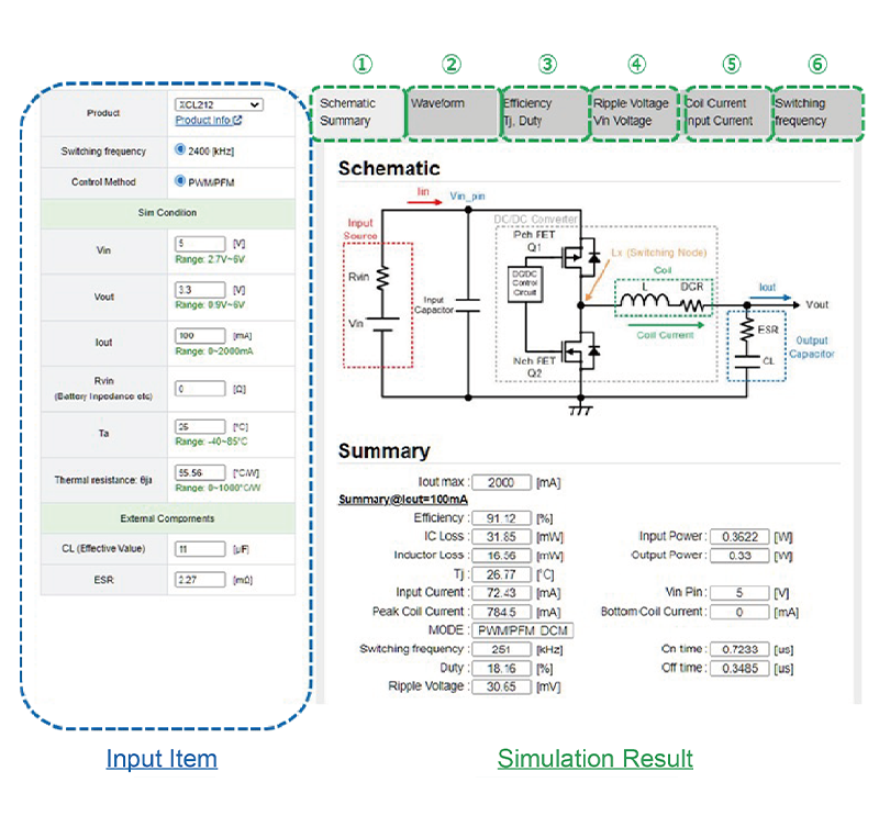
2. How to confirm the characteristics: "Summary" tab
Maximum output current
This is the maximum output current restricted by current limit, junction temperature, or maximum duty, etc.
With the step-up DC/DC converter, the maximum output current considerably varies depending on Vin/Vout, so confirmation of the maximum output current through simulation is very important. However, the simulation result shows a value based on TYP characteristic of IC, so the maximum output current under the worst condition is smaller than the simulation value (if you want to confirm the worst value, please contact TOREX separately).
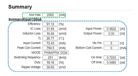
Summary
The summary collects various characteristics at the designated Iout.
It is possible to confirm characteristics under simulation conditions such as "efficiency", "loss", "junction temperature", "input current", "coil current", and "switching frequency".
3. How to confirm the characteristics: "Waveform" tab
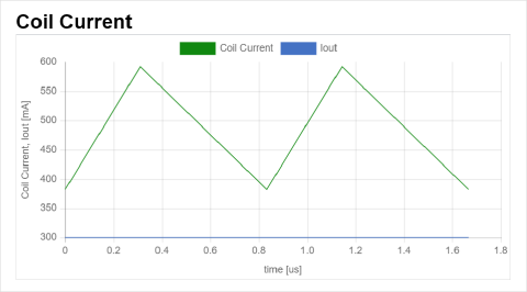
Coil Current
It is possible to confirm the coil current waveform at the designated Iout.
It is possible to mainly confirm peak current and bottom current of coil current.
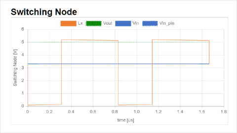
Switching Node (Lx waveform)
It is possible to confirm the switching node (Lx waveform) at the designated Iout.
This item is mainly used for confirmation of on time / off time and determination of control method (PWM control or PFM control) or operation mode (continuous mode or non-contiguous mode).
With this simulation, the ringing waveform in non-contiguous mode cannot be calculated. Consequently, a waveform without ringing is displayed.
4. How to confirm the characteristics: "Efficiency / Tj / Duty" tab
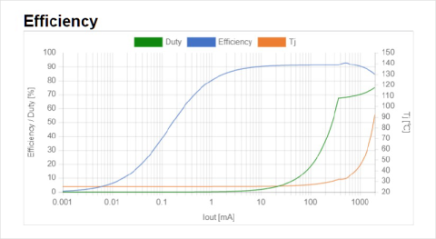
Efficiency / Junction Temperature (Tj) / Duty
It is possible to confirm one of the main characteristics of DC/DC converter, the efficiency.
As the estimated junction temperature is also displayed, you can confirm whether the junction temperature is within specification and whether an appropriate margin can be ensured.
It is possible to confirm duty too. This display can be utilized for confirming whether restrictions such as Max Duty limit is enforced.
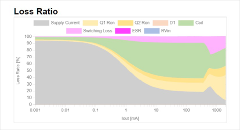
Loss Ratio
The percentage of where loss occurs in DC/DC is displayed.
It is possible to confirm the point where the loss occurs is IC or peripheral components and whether it is conduction loss or switching loss. Comprehending the loss ratio can determine whether the efficiency can be improved by changing peripheral components or constant number, etc.
5. How to confirm the characteristics: "Ripple Voltage / Vin Voltage" tab
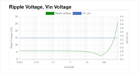
Ripple Voltage
This is the ripple voltage on output side that occurs at switching operation.
With this simulation, the ripple voltage that occurs in switching frequency cycle is displayed as an approximate value calculated from effective capacitance value of output capacitor and ESR.
Vin Pin Voltage
This is an input terminal voltage.
Input a resistance value to Rvin when giving consideration to resistance component such as ferrite bead / fuse that is inserted into internal impedance or input side of power storage device (battery / EDLC etc.). It is possible to confirm the degree of decrease of Vin pin voltage due to this resistance component and input voltage.
If the input item "Rvin" indicates 0Ω, Vin pin voltage = Vin.
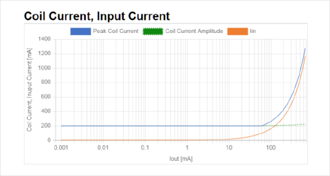
6. How to confirm the characteristics: "Coil Current / Input Current" tab
Coil Current
This is peak value and amplitude of coil current at each output current.
Input Current
This is the input current at each output current.
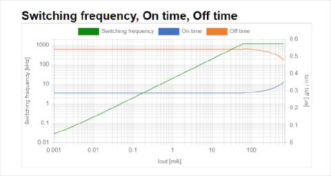
7. How to confirm the characteristics: "Switching frequency" tab
Switching frequency
This is the switching frequency at each output current.
This item is mainly utilized for confirming a rough indication of switching frequency at PFM and determining the switching current of PWM control and PFM control.
On time / Off time
FETTime of conduction to FET Q1 is displayed as on time. The conduction period of FET Q2 or SBD is displayed as off time.