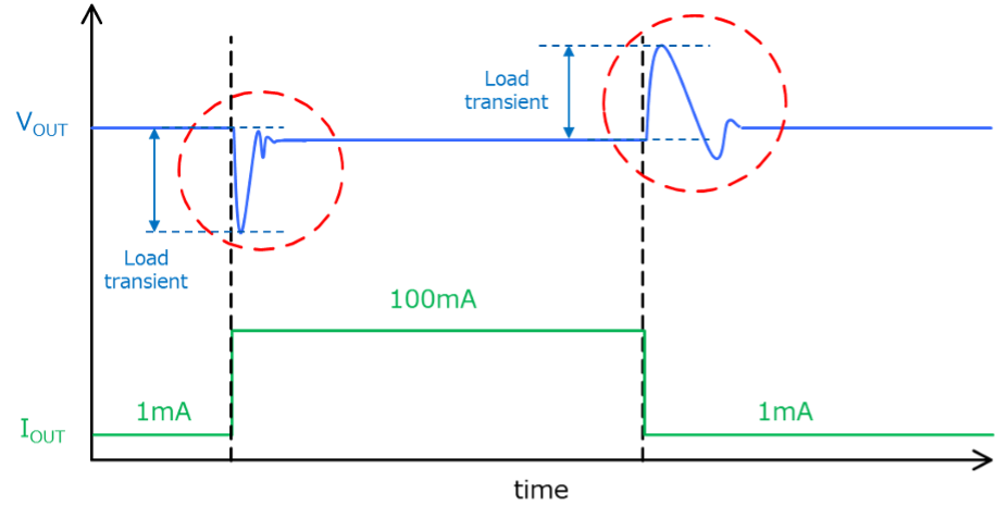
The load transient response characteristic is the output voltage fluctuation amount when the output current is transitionally (momentarily) changed.
The ideal load transient response characteristic keeps the output voltage change to a minimum while returning to the set voltage as quickly as possible.
The broken line on the left side of the following graph shows the output current increase from 1mA to 100mA and the resulting decrease in the output voltage.
The broken line on the right side shows the output current decrease from 100mA to 1mA and the corresponding increase in the output voltage (overshoot).
The voltage regulator load transient response characteristic is largely dependent on the IC’s current consumption.
The responses are largely divided into two types, "high current consumption and fast transient response" and "low current consumption but slow transient response”.
Let’s compare the transient response when the output current is 1mA to 50mA. Notice that in the two waveforms the vertical axis Vout range is different.
High Speed Type
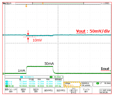
Current Consumption: 100μA
Low Consumption Type
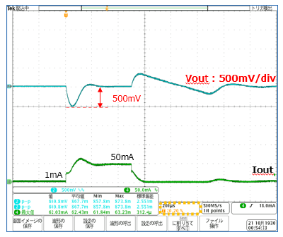
Current Consumption: 0.6μA
The left side high-speed type shows an output voltage decrease amount of 10mV. Compared to this, the low consumption type shows an output voltage decrease amount of 500mV, which is much larger than for the high-speed type.
In addition, for the time to return to the set voltage we can see that the high-speed type returns much quicker than does the low consumption type.
This is not simply an amount of change that is proportional to the current consumption value, but we can see there is a tendency for a difference in the transient response characteristic to appear in response to the current consumption value.
Here the operating principles of the voltage regulator will be used to explain why this large difference in the transient response characteristic between the high-speed type and the low consumption type occurs.
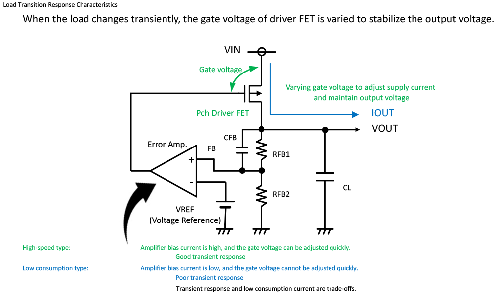
With the high-speed type, the current consumption is large, which allows it to quickly change the output of the error amplifier. This enables quick driver FET gate voltage control, making it possible to quickly change the driver FET on resistance. This operation makes it possible to obtain a fast transient response characteristic.
Conversely, with the low consumption type the output of the error amplifier cannot be changed quickly. For this reason, the driver FET gate voltage control is slow, which also makes the driver FET on resistance change slow. As a result, a fast response is not possible even when the output voltage is decreased by the transient change.
When the transient response characteristic is viewed as a “reaction speed,” to increase the speed the error amplifier current consumption must be increased, so the transient response and the current consumption are in a tradeoff relationship.