

In this article, we describe an overview of the DC/DC converter operation through the example of the "Continuous Current Mode (CCM)" for the step-down DC/DC converter in regard to the basic operation of the step-down DC/DC converter.
1.Basic structure of the step-down DC/DC converter
The step-down DC/DC converter is made up of the following major elements and electronic components to realize its voltage conversion function.
- Switching element (Main SW)
A power MOSFET is mainly used.
This element performs the role of supplying the coil current intermittently to the conductor by repeatedly switching on and off at high speed.
The on/off ratio (duty ratio) is an important element for deciding the output voltage. - Diode (D)
The diode is required for securing a path for the current to flow to the inductor when the switching element (SW) has turned off.
For asynchronous rectification, the Schottky diode is used. For synchronous rectification, a separate MOSFET is used instead of this diode, to reduce the power loss due to the forward voltage drop and achieve high efficiency. - Inductor (L)
Performs the role of supplying current to the output side by accumulating and releasing magnetic energy. - Input capacitor (CIN)
The input capacitor performs the role of stabilizing the DC/DC converter operation by reducing fluctuations in the input voltage. - Output capacitor (CL)
The output capacitor is used to stabilize the output voltage by absorbing the current supplied from the inductor.
2.Step-down DC/DC converter operation overview
The operation of the step-down DC/DC converter is achieved by repeatedly turning the switching element on and off at high speed in the following two phases.
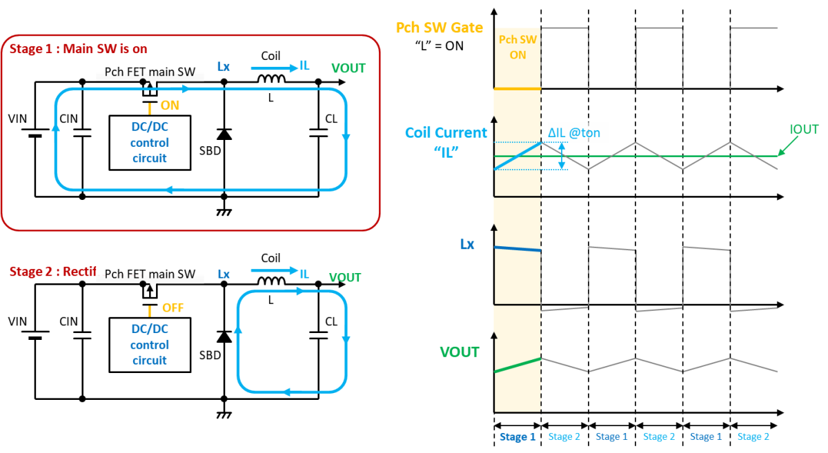
Stage 1: Pch FET switch on period
During this period, the Pch FET switch placed on the high side enters the on state.
When the Pch FET switch enters the on state, current flows from the input to the coil, and current is supplied to the output side.
The state of each node at this time is as follows.
- Pch FET gate: The gate voltage drops to a low level due to a signal from the control circuit, and the Pch FET switch is turned on. Due to this, VIN and the coil are connected.
- Current path: Current flows from the input voltage, passes through the Pch FET switch in the on state and the coil, and is supplied to the load connected to the output capacitance (CL).
- Coil current (IL): The positive voltage of the output voltage subtracted from the input voltage (Vin - Vout) is applied to the coil. Due to this voltage difference, the coil current increases linearly and the current increase ratio is (Vin - Vout)/L.
- Lx node: The Lx node that is the Pch FET drain is High (the voltage is close to VIN) because the switch is on.
- VOUT: The current is supplied through the coil, the output capacitor is charged, and the output voltage increases.
Stage 2: Pch FET switch off period
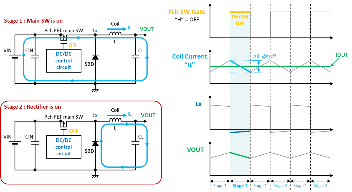
Next is the operation in stage 2 when the Pch FET switch is turned off.
During this period, the Pch FET switch placed on the high side is in the off state.
When the Pch FET switch enters the off state, current flows from GND to the coil, and current is supplied to the output side.
The state of each node at this time is as follows.
- Pch FET gate: The gate voltage rises to a high level due to a signal from the control circuit, and the Pch FET switch is turned off.
- Current path: Even if the switch is turned off, the inductor possesses a nature (Lenz's Law) that abhors sudden changing of the current. For that reason, the current accumulated in the inductor continues to flow through the diode (D) or the synchronous rectification MOSFET (SW2) to the output capacitor (CL).
- Coil current (IL): The negative voltage -Vout is applied to the coil. Due to this voltage difference, the coil current reduces linearly and the current increase ratio is -Vout/L.
- Lx node: To continue the coil current, the Schottky diode (or synchronous rectification MOSFET) generates the turn-on pressure through self-induction. Specifically, because the Lx pressure is lower than GND even, the diode is biased forward and a path is formed enabling the current to continue to flow.
- VOUT: The current is supplied through the coil, but because the supplied current is slightly less than the output current, the system is discharged and the output voltage falls.
3. Output voltage control: duty ratio
The control circuit always monitors the output voltage, and this duty ratio is adjusted in real time in accordance with fluctuations of the load current and the input voltage.
Due to this, however much the external conditions change, it is possible to maintain a stable target output voltage.
For example, if increasing the load current and reducing the output voltage is tried, the control circuit slightly increases the duty ratio, more energy is supplied to the output side, and the voltage is recovered.
Joined Torex Semiconductor in 2005.
After six years engaged in the development of power ICs such as DC/DC converters, worked for three years providing technical support for offline LED drivers.
Later took charge of technical support for Torex’s power IC customers.
With expertise gained through product development and extensive know-how accumulated from years of customer support — including solutions for power-related issues and troubleshooting — currently engaged in providing technical support and product proposals for Torex products.